Home / Academics / Featured Sites
Power Semiconductor Module Packaging and Testing Factory
Introduction
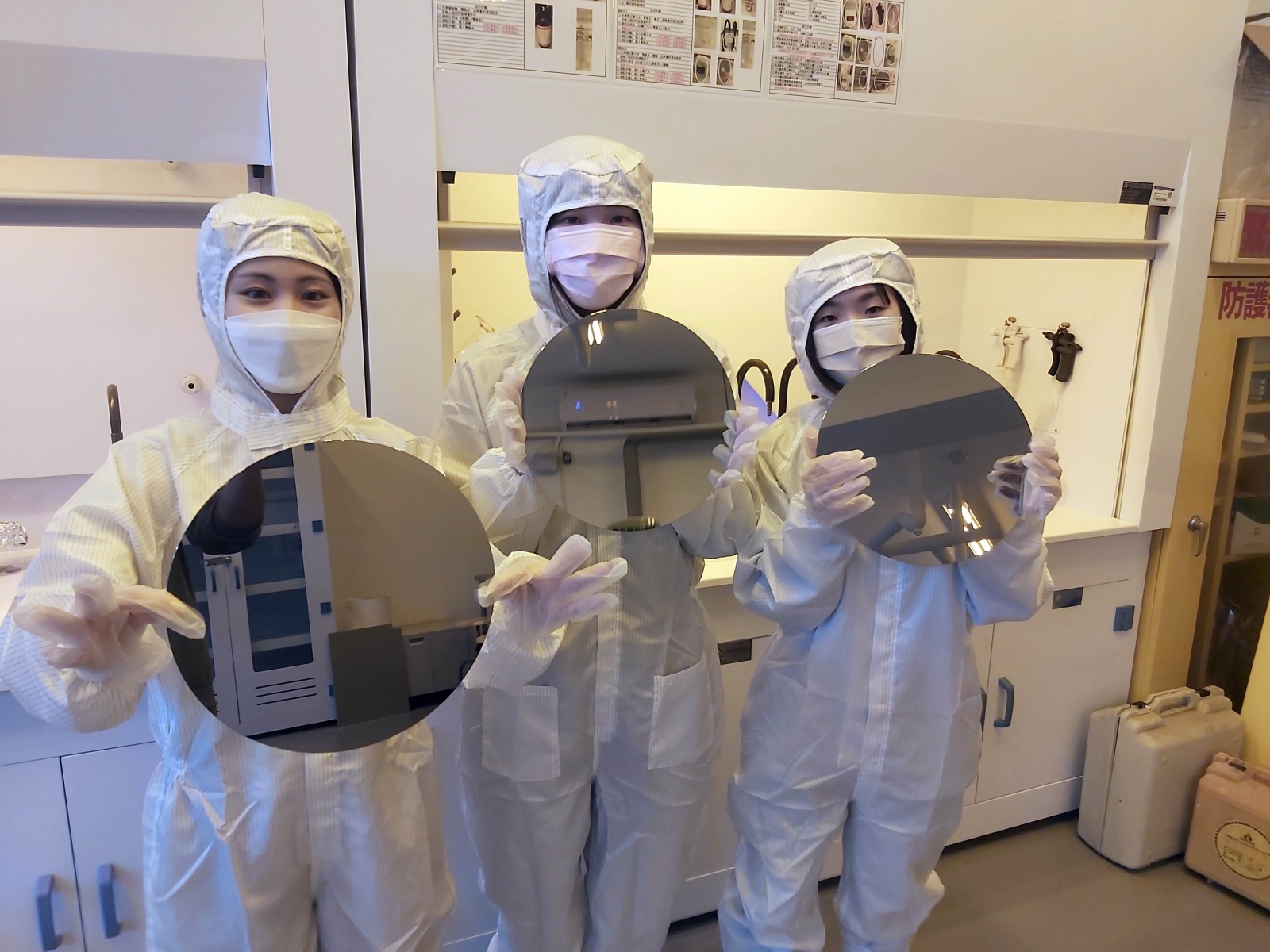
The university has devoted itself to cultivating technicians in semiconductor midstream and downstream sectors, including materials, processes, packaging, testing, and equipment, to meet the needs of semiconductor-related industries. The university has established a “Power Semiconductor Module Packaging and Testing Factory” and a “Semiconductor Components Process Center” to set up a complete packaging production line for the packaging of TVS diode SOD123 and SMA components for automotive electronics. The “Semiconductor Components Process Center” mainly focuses on training professionals and students in the semiconductor midstream manufacturing processes, including “oxidation,” “photolithography,” “etching,” “diffusion,” “metallization,” “point measurement,” “die dicing” and other practical processes of the semiconductor production process.
The goal is also to incorporate the government’s and industry-academia R&D plans, strengthen the connection with manufacturers, and train students to be familiar with the basic materials and midstream and downstream processes required for semiconductor production. Through these, the training will strengthen students’ professional skills and provide advanced technology courses and practical content to cultivate relevant talents and meet the needs of the industry.